2.262020
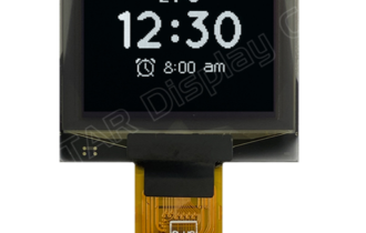
Winstar新製品 0.68 インチ COG 有機ELモジュール (Hotbar FPC)
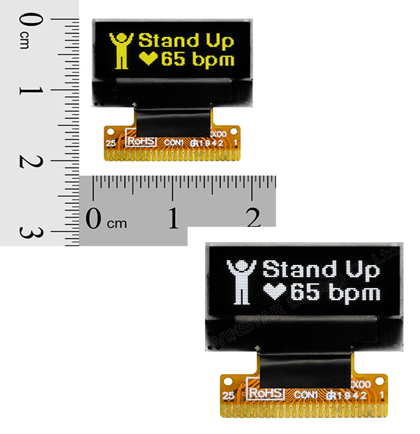
型番 WEO009632B-Hotbar
►タイプ: グラフィック有機ELモジュール
►結構: COG + Hotbar FPC
►サイズ: 0.68インチ
►96 x 32 ドットマトリックス
►SSD1305 コントローラー内蔵
►3V電源電圧
►1/32 duty
►インターフェース: 6800, 8080, SPI, I2C
►発光色: 白色 / 黄色
製品情報
WEO009632B-Hotbarバージョンは96×32解像度、対角サイズ0.68インチで作られたミニOLEDディスプレイで、SSD1305ドライバーICが組み込まれて、6800/8080 8ビットパラレル、I2C、及び4線SPIインターフェイスをサポートできます。この機種のロジックの供給電圧は3V、1/32駆動デューティで、50%チェックボード電流でのディスプレイは6mA @ 12Vcc(標準値)です。超薄型でバックライトが必要無しなOLEDディスプレイで、 軽量で低消費電力のタイプです。特 携帯機器、パーソナルケア機器、健康機器、メーター機器などに適しています。操作温度範囲は-40℃〜+80℃にして、保存温度範囲は-40℃〜+85℃にします。
外形図

製品仕様
ピン功能定義
| Pin No | 記号 | I/O | 功能 | |||||||||||||||
|---|---|---|---|---|---|---|---|---|---|---|---|---|---|---|---|---|---|---|
| 1 | N.C. | – | Reserved Pin(Supporting Pin) The supporting pins can reduce the influences from stresses on the function pins. These pins must be connected to external ground. |
|||||||||||||||
| 2,23 | VSS | P | Ground of Logic Circuit This is a ground pin. It also acts as a reference for the logic pins. It must be connected to external ground. |
|||||||||||||||
| 3,24 | VCC | P | Power Supply for OLED Panel This is the most positive voltage supply pin of the chip. It must be supplied externally. |
|||||||||||||||
| 4 | VCOMH | O | Voltage Output High Level for COM Signal This pin is the input pin for the voltage output high level for COM signals. A capacitor should be connected between this pin and VSS. |
|||||||||||||||
| 5 | IREF | I | Current Reference for Brightness Adjustment This pin is segment current reference pin. A resistor should be connected between this pin and VSS. Set the current lower than 10μA. |
|||||||||||||||
| 6 | D0~D7 | I/O | Host Data In put/ Output Bus These pins are 8-bit bi-directional data bus to be connected to the microprocessor’s data bus. When serial mode is selected, D1 will be the serial data input SDIN and D0 will be the serial clock input SCLK. When I2Cmode is selected, D2 & D1 should be tired together and serve as SDAout & SDAin in application and D0 is the serial clock input SCL. |
|||||||||||||||
| 7 | ||||||||||||||||||
| 8 | ||||||||||||||||||
| 9 | ||||||||||||||||||
| 10 | ||||||||||||||||||
| 11 | ||||||||||||||||||
| 12 | ||||||||||||||||||
| 13 | ||||||||||||||||||
| 14 | E(RD#) | I | Read/Write Enable or Read This pin is MCU interface input. When interfacing to a68XX-series microprocessor, this pin will be used as the Enable (E) signal. Read/write operation is initiated when this pin is pulled high and the CS# is pulled low. When connecting to an 80XX-microprocessor, this pin receives the Read (RD#) signal. Data read operation is initiated when this pin is pulled low and CS# is pulled low. |
|||||||||||||||
| 15 | R/W# (WR#) |
I | Read/ Write Selector Write This pin is MCU interface input. When interfacing to a68XX-series microprocessor, this pin will be used as Read/Write (R/W#) selection input. Pull this pin to “High” for read mode and pull it to “Low” for write mode. When 80XXinterface mode is selected, this pin will be the Write (WR#) input. Data write operation is initiated when this pin is pulled low and the CS# is pulled low. |
|||||||||||||||
| 16 | D/C# | I | Data/ Command Control This pin is Data/Command control pin. When the pin is pulled high, the input at D7~D0 is treated as display data. When the pin is pulled low, the input at D7~D0 will be transferred to the command register. For detail relationship to MCU interface signals, please refer to the Timing Characteristics Diagrams. When the pin is pulled high and serial interface mode is selected, the data at SDIN is treated as data. When it is pulled low, the data at SDIN will be transferred to the command register. In I2C mode, this pin acts as SA0 for slave address selection. |
|||||||||||||||
| 17 | RES# | I | Power Reset for Controller and Driver This pin is reset signal input. When the pin is low, initialization of the chip is executed. |
|||||||||||||||
| 18 | CS# | I | Chip Select This pin is the chip select input. The chip is enabled for MCU communication only when CS# is pulled low. |
|||||||||||||||
| 19 | BS2 | I | Communicating Protocol Select These pins are MCU interface selection input. See the following table:
Note |
|||||||||||||||
| 20 | BS1 | I | ||||||||||||||||
| 21 | VDDIO | P | Power supply for interface logic level. It should be match with MCU interface voltage level. VDDIO must always be equal or lower than VDD. |
|||||||||||||||
| 22 | VDD | P | Power Supply for Logic Circuit This is a voltage supply pin. It must be connected to external source. |
|||||||||||||||
| 25 | N.C. | – | Reserved Pin(Supporting Pin) The supporting pins can reduce the influences from stresses on the function pins. These pins must be connected to external ground. |
規格説明
| 項目 | 仕様 | 単位 |
|---|---|---|
| 解像度 | 96 × 32 | Dots |
| 外形寸法 | 19.80 × 12.32 × 1.21 (mm) | mm |
| 有効エリア | 16.298 × 5.418 (mm) | mm |
| ピクセルサイズ | 0.148 × 0.148 (mm) | mm |
| ピクセルピッチ | 0.17 × 0.17 (mm) | mm |
| 表示モード | パッシブマトリクス | |
| 発光色 | モノクロ | |
| 駆動方法 | 1/32 Duty | |
| IC | SSD1305 | |
| インターフェイス | 6800, 8080, SPI, I2C | |
| サイズ | 0.68 インチ | |
絶対最大定格
| パラメーター | 記号 | 最小値 | 最大値 | 単位 |
|---|---|---|---|---|
| ロジック電源電圧 | VDD | -0.3 | 4 | V |
| Display電源電圧 | VCC | 0 | 16 | V |
| 操作温度 | TOP | -40 | +80 | °C |
| 保存温度 | TSTG | -40 | +85 | °C |
電気特性
DC 特性
| 項目 | 記号 | 条件 | 最小値 | 典型値 | 最大値 | 単位 |
|---|---|---|---|---|---|---|
| ロジック電源電圧 | VDD | - | 2.8 | 3.0 | 3.3 | V |
| Display電源電圧 | VCC | - | 11.5 | 12 | 12.5 | V |
| 高レベル入力 | VIH | - | 0.8×VDD | - | VDD | V |
| 低レベル入力 | VIL | - | 0 | - | 0.2×VDD | V |
| 高レベル出力 | VOH | Iout = 100uA | 0.9×VDD | - | VDD | V |
| 低レベル出力 | VOL | Iout = 100uA | 0 | - | 0.1×VDD | V |
| 記号 | パラメーター | 最小値 | 典型値 | 最大値 | 単位 | 条件 |
|---|---|---|---|---|---|---|
| ICC | VCC Supply Current | – | 6 | 9 | mA | VDD =3.0V , Display 100% ON |
お問い合せはこちらから▶▶
関連記事
-

-

2022.11.25
電子黒板で何ができる?!シリーズ④ ご質問にお答えします
-

2018.12.10
Winstar 新商品 2.83 インチ 半透過TFT液晶モジュール 240×320
-

コメント
この記事へのトラックバックはありません。


トラスト・エレクトロニクス|表示器・サイネージ・CMコンテンツ・電子部品")
この記事へのコメントはありません。