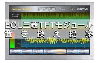
8.42020
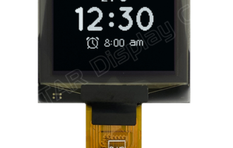
Winstar新製品 2.7インチ128×64 静電容量式タッチパネル 有機ELディスプレイ
型番 WEO012864Q-CTP
►タイプ: グラフィック有機ELディスプレイ
►結構: COG
►サイズ: 2.7インチ
►128 x 64 ドットマトリックス
►SSD1309コントローラー内蔵
►3V電源電圧
►1/64 duty
►インターフェース: 6800, 8080, SPI, I2C
►タッチパネル: 静電容量式タッチパネル
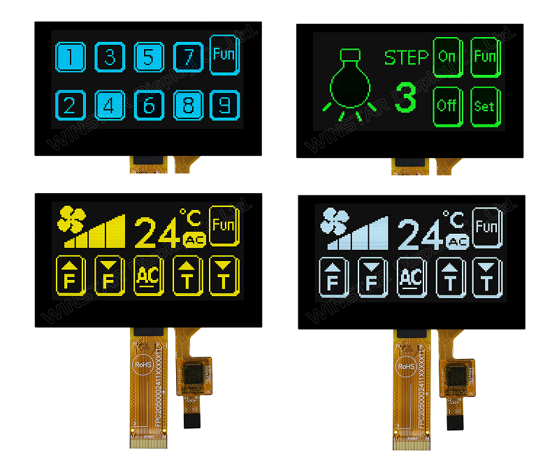
►発光色: 白色 / 黄色 / 空色 / 緑色
製品情報
WEO012864Q-CTP は2.7インチのグラフィック有機ELディスプレイで、静電容量式のタッチパネルを搭載しております。解像度は 128×64です。 SSD1309 ICを内蔵し、6800/8080 8ビットパラレル、4線式SPI・I2Cインターフェースをサポートできます。ロジック 電源電圧は2.8V~3.3Vで、標準値は3.0Vです。Display電源電圧は13Vで、デューティは 1/64 です。 WEO012864Q-CTPモジュールにGT911タッチパネルICを内蔵し、 I2Cインターフェースをサポートしており、静電容量方式タッチパネル(CTP)用の検出ポイントを内蔵しております。
この2.7インチの静電容量式タッチパネル付きWEO012864Q機種は スマートホームアプリケーション、 インテリジェントテクノロジーデバイス、エネルギーシステム、メーターデバイス、 通信システム、 医療機器などに適しております。 操作温度範囲は-20℃~+70℃で、 保存温度範囲は -30℃~+80℃です。
図面

製品仕様
ピン功能定義
| No. | 記号 | 説明 | |||||||||||||||
|---|---|---|---|---|---|---|---|---|---|---|---|---|---|---|---|---|---|
| 1 | NC(GND) | No connection | |||||||||||||||
| 2 | VLSS | This is an analog ground pin | |||||||||||||||
| 3 | VSS | Ground. | |||||||||||||||
| 4 | NC | No connection | |||||||||||||||
| 5 | VDD | Power supply pin for core logic operation | |||||||||||||||
| 6 | BS1 | MCU bus interface selection pins. Select appropriate logic setting as described in the following table. BS2 and BS1 are pin select
Note |
|||||||||||||||
| 7 | BS2 | ||||||||||||||||
| 8 | CS# | This pin is the chip select input connecting to the MCU. The chip is enabled for MCU communication only when CS# is pulled LOW (active LOW). |
|||||||||||||||
| 9 | RES# | This pin is reset signal input. When the pin is pulled LOW, initialization of the chip is executed. Keep this pin pull HIGH during normal operation. |
|||||||||||||||
| 10 | D/C# | This pin is Data/Command control pin connecting to the MCU. When the pin is pulled HIGH, the data at D[7:0] will be interpreted as data. When the pin is pulled LOW, the data at D[7:0] will be transferred to a command register. In I2C mode, this pin acts as SA0 for slave address selection. |
|||||||||||||||
| 11 | R/W# | This pin is read / write control input pin connecting to the MCU interface. When 6800 interface mode is selected, this pin will be used as Read/Write (R/W#) selection input. Read mode will be carried out when this pin is pulled HIGH and write mode when LOW. When 8080 interface mode is selected, this pin will be the Write (WR#) input. Data write operation is initiated when this pin is pulled LOW and the chip is selected. When serial or I2C interface is selected, this pin must be connected to VSS. |
|||||||||||||||
| 12 | E/RD# | This pin is MCU interface input. When 6800 interface mode is selected, this pin will be used as the Enable (E) signal. Read/write operation is initiated when this pin is pulled HIGH and the chip is selected. When 8080 interface mode is selected, this pin receives the Read (RD#) signal. Read operation is initiated when this pin is pulled LOW and the chip is selected. When serial or I2C interface is selected, this pin must be connected to VSS. |
|||||||||||||||
| 13-20 | D0~D7 | These pins are bi-directional data bus connecting to the MCU data bus. Unused pins are recommended to tie LOW. When serial interface mode is selected, D0 will be the serial clock input: SCLK; D1 will be the serial data input: SDIN and D2 should be kept NC. When I2C mode is selected, D2, D1 should be tied together and serve as SDAout, SDAin in application and D0 is the serial clock input, SCL. |
|||||||||||||||
| 21 | IREF | This pin is the segment output current reference pin. IREF is supplied externally. |
|||||||||||||||
| 22 | VCOMH | COM signal deselected voltage level. A capacitor should be connected between this pin and VSS. |
|||||||||||||||
| 23 | VCC | Power supply for panel driving voltage. This is also the most positive power voltage supply pin. | |||||||||||||||
| 24 | NC(GND) | No connection |
CTP PIN 定義
| No. | 記号 | 説明 |
|---|---|---|
| 1 | GND | Power ground |
| 2 | VDD | Power supply |
| 3 | INT | Interrupt signal, active low, asserted to request Host start a new transaction |
| 4 | SDA | I2C data signal |
| 5 | SCL | I2C clock signal |
| 6 | RST | External reset signal, active low |
| 7 | GND | Power ground |
| 8 | GND | Power ground |
| 9 | GND | Power ground |
| 10 | GND | Power ground |
規格説明
| 項目 | 仕様 | 単位 |
|---|---|---|
| ドットマトリックス(解像度) | 128 x 64 | - |
| モジュールサイズ | 74.8 × 44.16 × 3.66 | mm |
| 有効エリア | 61.41 × 30.69 | mm |
| ドットサイズ | 0.45 × 0.45 | mm |
| ドットピッチ | 0.48 × 0.48 | mm |
| 表示モード | パッシブマトリクス | |
| 発光色 | モノクロ | |
| 駆動方法 | 1/64 Duty | |
| IC | SSD1309 | |
| インターフェイス | 6800,8080,4-Wire SPI,I2C | |
| 表示サイズ | 2.7インチ | |
| CTP IC | GT911 | |
| Detect Point | 1 | |
| CTP インターフェイス | I2C | |
| 表面処理 | グレア | |
絶対最大定格
絶対最大定格
| パラメーター | 記号 | 最小値 | 最大値 | 単位 |
|---|---|---|---|---|
| ロジック電源電圧 | VDD | -0.3 | 4 | V |
| Display電源電圧 | VCC | 0 | 15 | V |
| 操作温度 | TOP | -20 | +70 | °C |
| 保存温度 | TSTG | -30 | +80 | °C |
タッチパネルコントローラー GT911
| パラメーター | 記号 | 最小値 | 最大値 | 単位 |
|---|---|---|---|---|
| 電源電圧 | VDD | 2.66 | 3.47 | V |
電気特性
DC電気特性
| 項目 | 記号 | 条件 | 最小値 | 典型値 | 最大値 | 単位 |
|---|---|---|---|---|---|---|
| ロジック電源電圧 | VDD | - | 2.8 | 3.0 | 3.3 | V |
| Display電源電圧 | VCC | - | 12.5 | 13 | 13.5 | V |
| 高レベル入力 | VIH | - | 0.8×VDD | - | - | V |
| 低レベル入力 | VIL | - | - | - | 0.2×VDD | V |
| 高レベル出力 | VOH | - | 0.9×VDD | - | - | V |
| 低レベル出力 | VOL | - | - | - | 0.1×VDD | V |
| 50% Check Board operating Current | VCC =13.0V | 20 | 30 | 50 | mA | |
タッチパネルコントローラー GT911
| 項目 | 記号 | 最小値 | 典型値 | 最大値 | 単位 |
|---|---|---|---|---|---|
| 電源電圧 | VDD | 2.8 | 3.0 | 3.3 | V |
| 高レベル入力 | VIH | 0.75xVDD | VDD+0.3 | V | |
| 低レベル入力 | VIL | -0.3 | - | 0.25xVDD | V |
| 高レベル出力 | VOH | 0.85xVDD | - | - | V |
| 低レベル出力 | VOL | - | - | 0.15xVDD | V |
関連記事


コメント
この記事へのトラックバックはありません。


トラスト・エレクトロニクス|表示器・サイネージ・CMコンテンツ・電子部品")
この記事へのコメントはありません。