2.252022
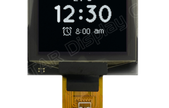
Winstara新製品 128×64 静電容量式タッチパネル OLEDモジュール
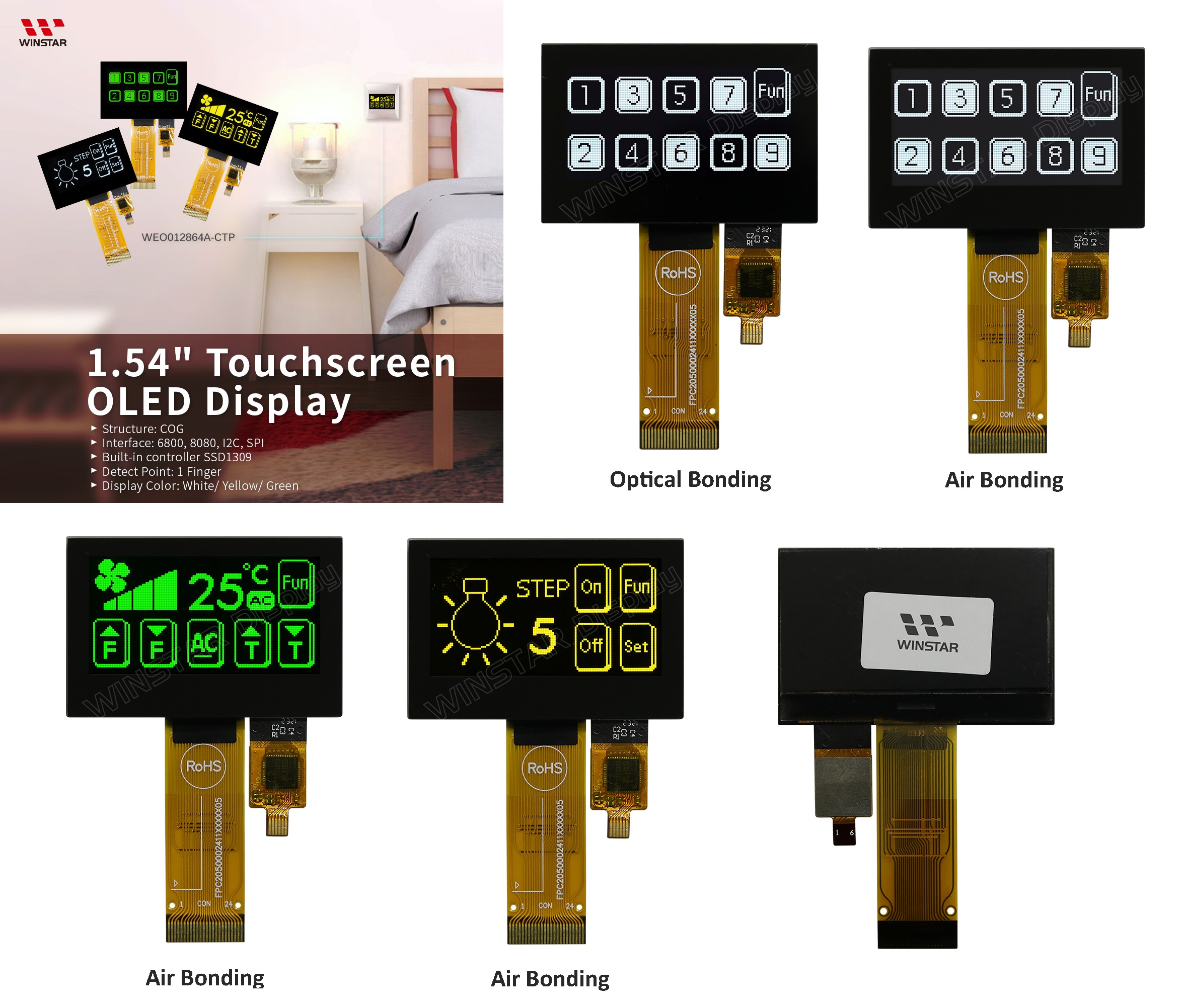
型番 WEO012864A-CTP
►タイプ: グラフィック有機ELディスプレイ
►結構: COG ►サイズ: 1.54インチ
►128 x 64 ドットマトリックス
►SSD1309コントローラー内蔵
►3V電源電圧 ►1/64 duty
►インターフェース: 6800,8080,SPI,I2C
►静電容量式タッチパネル(CTP); オプション OCA CTP
►検出ポイント: 1 ►発光色: 白色 / 黄色 / 緑色
製品情報
WEO012864A-CTPはモジュールに静電容量式タッチパネルを備えた1.54インチCOG構造のグラフィック有機ELディスプレイで、解像度は128×64ピクセルです。このモジュールはSSD1309 ICが組み込まれ、 6800/8080 8ビットパラレルにして、4線式SPI及びI2Cインターフェースを介して通信できます。 ロジックの供給電圧は2.8Vから3.3V、標準値は3.0Vで、ディスプレイの供給電圧は12.5V、駆動デューティ 1/64です。
このWEO012864A-CTPモデルには2つのCTPオプションがあります。 1つのCTPタッチパネルは、エアボンディングプロセスによるもので、もう1つのCTPオプションはオプティカルボンディング(OCA)プロセスによるものです。これらの2つのCTPタッチパネルオプションは両方ともFT6336U ICに組み込まれており、1つの検出ポイントでI2Cインターフェースをサポートします。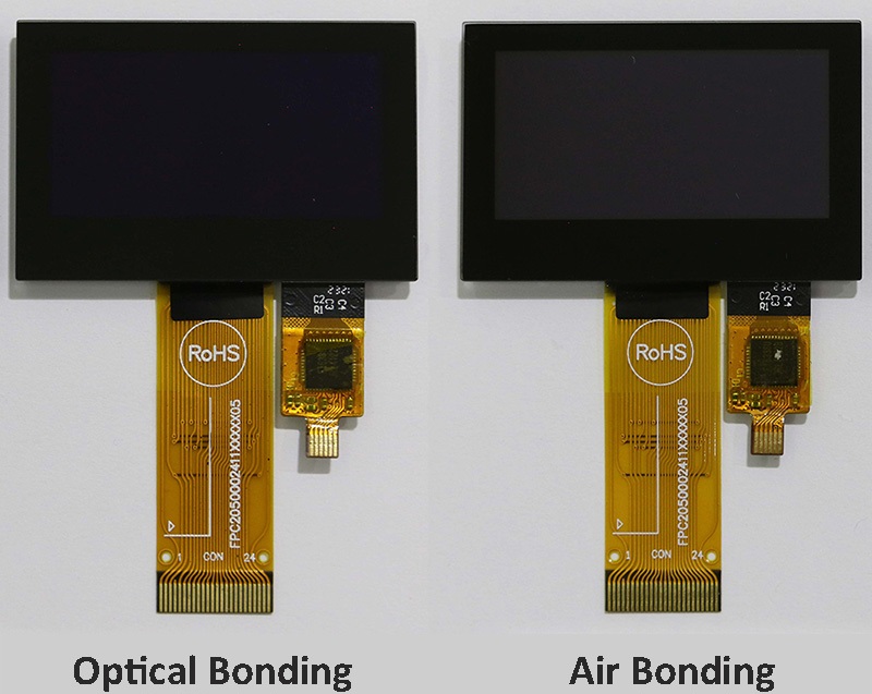
CTPモデルを備えたWEO012864Aはスマートホームアプリケーション、インテリジェントテクノロジーデバイス、メーターデバイス、産業用制御システム、医療機器等に最適です。このモジュールの操作温度範囲は-10℃~+60℃で、保存温度範囲は-20℃~+70℃です。
図 面

製品仕様
Interface Pin Function
| No. | 記号 | 説明 | |||||||||||||||
|---|---|---|---|---|---|---|---|---|---|---|---|---|---|---|---|---|---|
| 1 | NC(GND) | No connection | |||||||||||||||
| 2 | VLSS | This is an analog ground pin | |||||||||||||||
| 3 | VSS | Ground. | |||||||||||||||
| 4 | NC | No connection | |||||||||||||||
| 5 | VDD | Power supply pin for core logic operation | |||||||||||||||
| 6 | BS1 | MCU bus interface selection pins. Select appropriate logic setting as described in the following table. BS2 and BS1 are pin select
Note |
|||||||||||||||
| 7 | BS2 | ||||||||||||||||
| 8 | CS# | This pin is the chip select input connecting to the MCU. The chip is enabled for MCU communication only when CS# is pulled LOW (active LOW). |
|||||||||||||||
| 9 | RES# | This pin is reset signal input. When the pin is pulled LOW, initialization of the chip is executed. Keep this pin pull HIGH during normal operation. |
|||||||||||||||
| 10 | D/C# | This pin is Data/Command control pin connecting to the MCU. When the pin is pulled HIGH, the data at D[7:0] will be interpreted as data. When the pin is pulled LOW, the data at D[7:0] will be transferred to a command register. In I2C mode, this pin acts as SA0 for slave address selection. |
|||||||||||||||
| 11 | R/W# | This pin is read / write control input pin connecting to the MCU interface. When 6800 interface mode is selected, this pin will be used as Read/Write (R/W#) selection input. Read mode will be carried out when this pin is pulled HIGH and write mode when LOW. When 8080 interface mode is selected, this pin will be the Write (WR#) input. Data write operation is initiated when this pin is pulled LOW and the chip is selected. When serial or I2C interface is selected, this pin must be connected to VSS. |
|||||||||||||||
| 12 | E/RD# | This pin is MCU interface input. When 6800 interface mode is selected, this pin will be used as the Enable (E) signal. Read/write operation is initiated when this pin is pulled HIGH and the chip is selected. When 8080 interface mode is selected, this pin receives the Read (RD#) signal. Read operation is initiated when this pin is pulled LOW and the chip is selected. When serial or I2C interface is selected, this pin must be connected to VSS. |
|||||||||||||||
| 13-20 | D0~D7 | These pins are bi-directional data bus connecting to the MCU data bus. Unused pins are recommended to tie LOW. When serial interface mode is selected, D0 will be the serial clock input: SCLK; D1 will be the serial data input: SDIN and D2 should be kept NC. When I2C mode is selected, D2, D1 should be tied together and serve as SDAout, SDAin in application and D0 is the serial clock input, SCL. |
|||||||||||||||
| 21 | IREF | This pin is the segment output current reference pin. IREF is supplied externally. |
|||||||||||||||
| 22 | VCOMH | COM signal deselected voltage level. A capacitor should be connected between this pin and VSS. |
|||||||||||||||
| 23 | VCC | Power supply for panel driving voltage. This is also the most positive power voltage supply pin. | |||||||||||||||
| 24 | NC(GND) | No connection |
CTP ピン功能
| 1 | GND | Ground |
| 2 | VDD | Power Supply Voltage of CTP |
| 3 | RST | External Reset, Low is active |
| 4 | INT | External interrupt to the host |
| 5 | SCL | I2C clock input |
| 6 | SDA | I2C data input and output |
規格説明
| 項目 | 仕様 | 単位 |
|---|---|---|
| ドットマトリックス(解像度) | 128 x 64 | - |
| モジュールサイズ | 43.04 × 28.22 × 3.01 | mm |
| 有効エリア | 35.05 × 17.51 | mm |
| ドットサイズ | 0.249 × 0.249 | mm |
| ドットピッチ | 0.274 × 0.274 | mm |
| 表示モード | パッシブマトリックス | |
| 発光色 | モノクロ | |
| 駆動方法 | 1/64 Duty | |
| IC | SSD1309 | |
| インターフェイス | 6800,8080,4-wire SPI,I2C | |
| 表示サイズ(対角線) | 1.54 インチ | |
| CTP IC | FT6336U | |
| 検出ポイント | 1 | |
| CTP インターフェイス | I2C | |
| 表面処理 | グレア | |
絶対最大定格
| パラメーター | 記号 | 最小値 | 最大値 | 単位 |
|---|---|---|---|---|
| ロジック電源電圧 | VDD | -0.3 | 4 | V |
| Display電源電圧 | VCC | 0 | 17 | V |
| 操作温度 | TOP | -10 | +60 | °C |
| 保存温度 | TSTG | -20 | +70 | °C |
タッチパネルコントローラー FT6336U
| パラメーター | 記号 | 最小値 | 最大値 | 単位 |
|---|---|---|---|---|
| 電源電圧 | VDD | 0 | 3.6 | V |
電気特性
DC電気特性
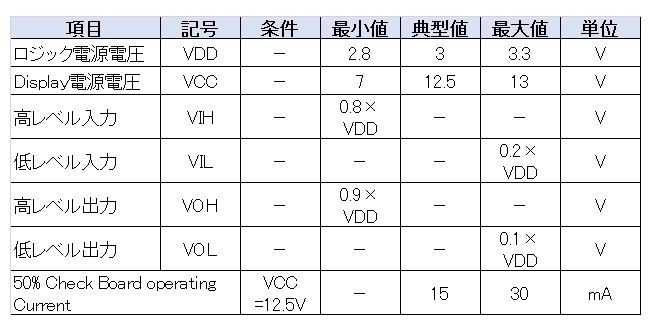
タッチパネルコントローラー FT6336U
| 項目 | 記号 | 条件 | 最小値 | 典型値 | 最大値 | 単位 |
|---|---|---|---|---|---|---|
| 電源電圧 | VDD | - | 2.8 | 3.0 | 3.3 | V |
| 高レベル入力 | VIH | - | 0.7×VDD | - | VDD | V |
| 低レベル入力 | VIL | - | -0.3 | - | 0.3×VDD | V |
| 高レベル出力 | VOH | - | 0.7×VDD | - | - | V |
| 低レベル出力 | VOL | - | - | - | 0.3×VDD | V |
|
||
| 型 番 | WEO012864AWPP3A00000 | WEO012864AWPP3D00001 |
| OLED IC | SSD1309 | SSD1309 |
| OLED インターフェイス | 6800,8080,4-wire SPI,I2C | 6800,8080,4-wire SPI,I2C |
| TP IC | FT6336U | FT6336U |
| TP インターフェイス | I2C | I2C |
| TP 検出ポイント | 1 | 1 |
| TP bonding method | OCA Optical-Bonding | Air-Bonding |
関連記事
-

-

2019.2.12
Winstar 新商品 7インチ広視野角,広温,超高輝度 TFT LCD
-

-

2022.5.12
Winstar 製品 4.3インチ 静電容量タッチパネル TFT IPS 液晶
コメント
この記事へのトラックバックはありません。


トラスト・エレクトロニクス|表示器・サイネージ・CMコンテンツ・電子部品")
この記事へのコメントはありません。