2.62023
Winstar製品 キャラクター 20×4 COG LCDモジュール
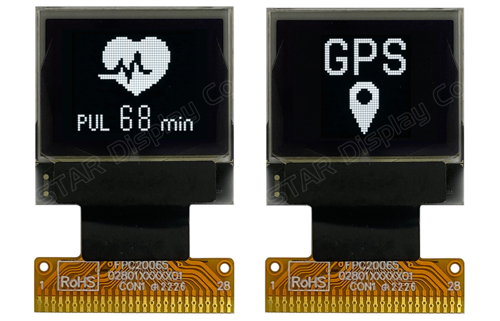
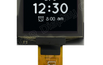
型番 WEO006448B
►0.66インチ OLED
►グラフィック液晶有機モジュール
►結構: COG
►64 x 48 ドットマトリックス
►SSD1315 コントローラー内蔵
►3V電源電圧
►1/48 duty
►インターフェース: 6800, 8080, 4-Wire SPI, I2C
►発光色: 白色
製品情報
WEO006448Bはコンシューマーグレードの COG OLED ディスプレイで、0.66 インチ、解像度 64×48 ドットで構成され、SSD1315 IC が組み込まれたモジュールです。6800、8080、4 線式 SPI、および I2C インターフェイスをサポートしております。 ロジック電源電圧は 3V、ディスプレイ電源電圧は 7.5Vです。50%チェックボード表示での電流は3mA @7.5V VCC (標準値)で、駆動デューティは 1/48 です。内部チャージポンプ電源と外部 VCC 電源をサポートしております。その動作及び保管温度範囲は-30℃~+70℃です。ウェアラブル デバイス、ポータブル デバイスなどに適されております。
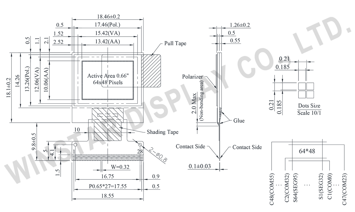
図 面
製品仕様
ピン功能定義
| No. | 記号 | 説明 | |||||||||||||||
|---|---|---|---|---|---|---|---|---|---|---|---|---|---|---|---|---|---|
| 1 | ESD_GND | It should be connected to ground. | |||||||||||||||
| 2 | C2N | C1P/C1N – Pin for charge pump capacitor; Connect to each other with a capacitor. C2P/C2N – Pin for charge pump capacitor; Connect to each other with a capacitor. |
|||||||||||||||
| 3 | C2P | ||||||||||||||||
| 4 | C1P | ||||||||||||||||
| 5 | C1N | ||||||||||||||||
| 6 | VBAT | Power supply for charge pump regulator circuit.
|
|||||||||||||||
| 7 | VSS | This is a ground pin. | |||||||||||||||
| 8 | VDD | Power supply pin for core logic operation. | |||||||||||||||
| 9 | BS1 | These pins are MCU interface selection input. See the following table.
|
|||||||||||||||
| 10 | BS2 | ||||||||||||||||
| 11 | CS# | The chip is enabled for MCU communication only when CS# is pulled LOW (active LOW). | |||||||||||||||
| 12 | RES# | This pin is reset signal input. When the pin is low, initialization of the chip is executed. Keep this pin HIGH (i.e. connect to VDD) during normal operation. | |||||||||||||||
| 13 | D/C# | This pin is Data/Command control pin connecting to the MCU. When the pin is pulled HIGH, the data at D[7:0] will be interpreted as data. When the pin is pulled LOW, the data at D[7:0] will be transferred. |
|||||||||||||||
| 14 | R/W# | This is read / write control input pin connecting to the MCU interface. When interfacing to a 6800-series microprocessor, this pin will be used as Read/Write (R/W#) selection input. Read mode will be carried out when this pin is pulled HIGH (i.e. connect to VDD) and write mode when LOW. When 8080 interface mode is selected, this pin will be the Write (WR#) input. Data write operation is initiated when this pin is pulled LOW and the chip is selected. When serial or I2C interface is selected, this pin must be connected to VSS. |
|||||||||||||||
| 15 | E/RD# | This pin is MCU interface input. When 6800 interface mode is selected, this pin will be used as the Enable (E) signal. Read/write operation is initiated when this pin is pulled HIGH and the chip is selected. When 8080 interface mode is selected, this pin receives the Read (RD#) signal. Read operation is initiated when this pin is pulled LOW and the chip is selected. When serial or I2C interface is selected, this pin must be connected to VSS |
|||||||||||||||
| 16~23 | D0~D7 | These are 8-bit bi-directional data bus to be connected to the microprocessor’s data bus. When serial interface mode is selected, D0 will be the serial clock input: SCLK; D1 will be the serial data input: SDIN. When I2C mode is selected, D2, D1 should be tied together and serve as SDAout, SDAin in application and D0 is the serial clock input, SCL . | |||||||||||||||
| 24 | IREF | This is segment output current reference pin. When external IREF is used, a resistor should be connected between this pin and VSS to maintain the IREF current at 30uA. When internal IREF is used, this pin should be kept NC. |
|||||||||||||||
| 25 | VCOMH | COM signal deselected voltage level. A capacitor should be connected between this pin and VSS. |
|||||||||||||||
| 26 | VCC | Power supply for panel driving voltage. This is also the most positive power voltage supply pin When charge pump is enabled, a capacitor should be connected between this pin and VSS. |
|||||||||||||||
| 27 | VLSS | This is an analog ground pin. It should be connected to VSS externally. | |||||||||||||||
| 28 | ESD GND | It should be connected to ground. |
規格説明
| 項目 | 仕様 | 単位 |
|---|---|---|
| ドットマトリックス(解像度) | 64 x 48 Dots | – |
| モジュールサイズ | 18.46 × 18.10 × 1.26 | mm |
| 有効エリア | 13.42 × 10.06 | mm |
| ドットサイズ | 0.185 × 0.185 | mm |
| ドットピッチ | 0.210 × 0.210 | mm |
| 表示モード | Passive Matrix | |
| 発光色 | Monochrome | |
| 駆動方法 | 1/48 Duty | |
| IC | SSD1315 | |
| インターフェイス | 6800, 8080, 4-Wire SPI, I2C | |
| 表示サイズ(対角線) | 0.66 inch | |
絶対最大定格
| パラメーター | 記号 | 最小值 | 最大值 | 単位 |
|---|---|---|---|---|
| 電源電圧 | VDD | 0 | 4.0 | V |
| チャージポンプレギュレータ供給電圧 | VBAT | 0 | 6.0 | V |
| Display電源電圧 | VCC | 0 | 18.0 | V |
| 操作温度 | TOP | -30 | +70 | °C |
| 保存温度 | TSTG | -30 | +70 | °C |
電気特性
| 項目 | 記号 | 条件 | 最小值 | 典型值 | 最大值 | 単位 |
|---|---|---|---|---|---|---|
| ロジック電源電圧 | VDD | - | 1.65 | 3.0 | 3.3 | V |
| 表示用電源電圧(外部供給) | VCC | - | 6.0 | 7.5 | 15.0 | V |
| チャージポンプレギュレータ供給電圧 | VBAT | - | 3.0 | 3.3 | VDD | V |
| 用於顯示的電荷泵輸出電壓(由內部 DC/DC 生成) | - | 7.0 | 7.5 | 0.2×VDD | V | |
| 入力電圧(High) | VIH | - | 0.8×VDD | - | VDD | V |
| 入力電圧(Low) | VIL | - | 0 | - | 0.1×VDD | V |
| 出力電圧(High) | VOH | – | 0.9×VDD | – | 30 | V |
| 出力電圧(Low) | VOL | – | 0 | – | 30 | V |
| ディスプレイ 50% ピクセルオン (外部から供給される VCC) | ICC | VCC=7.5V | - | 3 | 30 | mA |
| ディスプレイ 50% ピクセルオン (内部 DC/DC によって生成される VCC) | IBAT | – | - | 15 | 30 | mA |
関連記事
-

2020.7.20
新時代 IoTデジタルサイネージのご紹介
-

-

-


トラスト・エレクトロニクス|表示器・サイネージ・CMコンテンツ・電子部品")