10.62020
Winstar新製品 128×64 グラフィック COG 液晶表示器
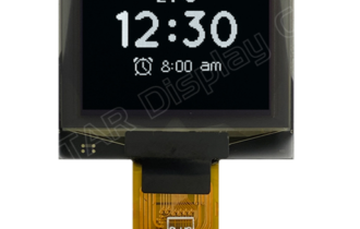
型番 WO12864K
►COGタイプのLCDモジュール
►グラフィックディスプレイ
►解像度(W×H)ドット: 128×64
►ST7565V コントローラー内蔵
►3V電源電圧 ►1/65 duty cycle, 1/9 bias
►インターフェース: 6800/8080/SPI
製品情報
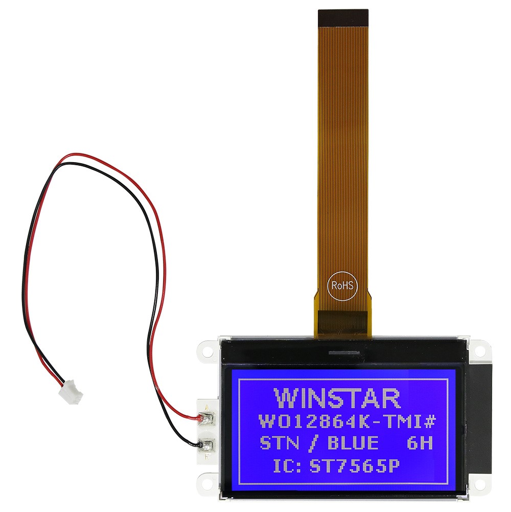
WO12864K/WO12864K1はモノクロのCOG構造のグラフィック LCD ディスプレイです。ST7565 ICを内蔵し、8-ビット 6800・ 8-ビット8080 パラレルと4線式 SPI インターフェースをサポート致します。 電源電圧は3Vで、VOPは 9.5Vで、デューティは 1/65です。 WO12864K は 負電圧のST7565V IC を内蔵し、WO12864K1は正電圧のST7565P IC を内蔵しております。
WO12864K/K1はネガティブ 表示・青色透過型パネルと白色LED の仕様を提供致します。 他のLCD/LEDの発光色の組み合わせが必要であれば、担当窓口にご相談ください。
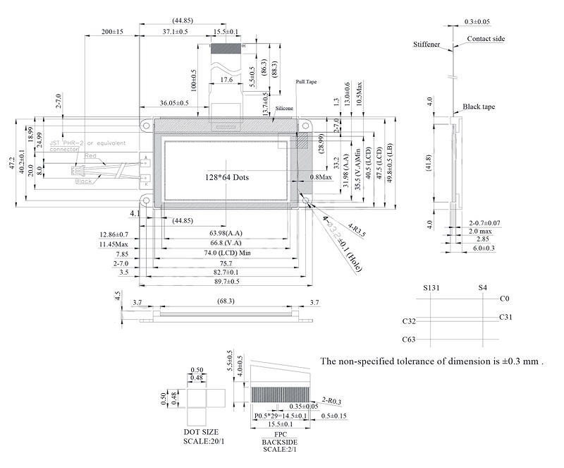
図 面
製品仕様
ピン功能定義
| Pin No. | 記号 | 説明 |
|---|---|---|
| 1 | /CS1 | This is the chip select signal. When /CS1 = “L”, then the chip select becomes active, and data/command I/O is enabled. |
| 2 | /RES | I When /RES is set to “L,” the settings are initialized. The reset operation is performed by the /RES signal level. |
| 3 | A0 | This is connect to the least significant bit of the normal MPU address bus, and it determines whether the data bits are data or a command. A0 = “H”: Indicates that D0 to D7 are display data. A0 = “L”: Indicates that D0 to D7 are control data |
| 4 | /WR | • When connected to an 8080 MPU, this is active LOW. (R/W) This terminal connects to the 8080 MPU /WR signal. The signals on the data bus are latched at the rising edge of the /WR signal. • When connected to a 6800 Series MPU: This is the read/write control signal input terminal. When R/W = “H”: Read. When R/W = “L”: Write. |
| 5 | /RD | • When connected to an 8080 MPU, this is active LOW. (E) This pin is connected to the /RD signal of the 8080 MPU, and the ST7565V series data bus is in an output status when this signal is “L”. • When connected to a 6800 Series MPU, this is active HIGH. This is the 6800 Series MPU enable clock input terminal. |
| 6 | D0 | This is an 8-bit bi-directional data bus that connects to an 8-bit or 16-bit standard MPU data bus. When the serial interface is selected (P/S = “L”) : D7 : serial data input (SI) ; D6 : the serial clock input (SCL). D0 to D5 are set to high impedance. When the chip select is not active, D0 to D7 are set to high impedance. |
| 7 | D1 | |
| 8 | D2 | |
| 9 | D3 | |
| 10 | D4 | |
| 11 | D5 | |
| 12 | D6 | |
| 13 | D7 | |
| 14 | VDD | Shared with the MPU power supply terminal Vcc. |
| 15 | GND | This is a 0V terminal connected to the system GND. |
| 16 | VOUT | DC/DC voltage converter. Connect a capacitor between this terminal and VSS. |
| 17 | CAP3- | DC/DC voltage converter. Connect a capacitor between this terminal and the CAP1+ terminal. |
| 18 | CAP1+ | DC/DC voltage converter. Connect a capacitor between this terminal and the CAP1- terminal. |
| 19 | CAP1- | DC/DC voltage converter. Connect a capacitor between this terminal and the CAP1+ terminal. |
| 20 | CAP2- | DC/DC voltage converter. Connect a capacitor between this terminal and the CAP2- terminal. |
| 21 | CAP2+ | DC/DC voltage converter. Connect a capacitor between this terminal and the CAP2+ terminal. |
| 22 | V1 | This is a multi-level power supply for the liquid crystal drive. The voltage Supply applied is determined by the liquid crystal cell, and is changed through the use of are sistive voltage divided or through changing the impedance using an op. amp. Voltage levels are determined based on VDD, |
| 23 | V2 | |
| 24 | V3 | |
| 25 | V4 | |
| 26 | V5 | |
| 27 | VR | Output voltage regulator terminal. Provides the voltage between VDD and V5 through a resistive voltage divider. IRS = “L” : the V5 voltage regulator internal resistors are not used . IRS = “H” : the V5 voltage regulator internal resistors are used . |
| 28 | C86 | This is the MPU interface switch terminal. C86 = “H”: 6800 Series MPU interface. C86 = “L”: 8080 MPU interface. |
| 29 | P/S | This is the parallel data input/serial data input switch terminal. P/S = “H”: Parallel data input. P/S = “L”: Serial data input. When P/S = “L”, D0 to D5 fixed “H”. /RD (E) and /WR (R/W) are fixed to either “H” or “L”. With serial data input, It is impossible read data from RAM . |
| 30 | IRS | This terminal selects the resistors for the V5 voltage level adjustment. IRS = “H”: Use the internal resistors IRS = “L”: Do not use the internal resistors. The V5 voltage level is regulated by an external resistive voltage divider attached to the VR terminal |
規格説明
| 項目 | 仕様 | 単位 |
|---|---|---|
| ドットマトリックス(解像度) | 128 x 64 | - |
| モジュールサイズ | 89.7 x 49.8 x 6.0 | mm |
| 表示エリア | 66.8 x 35.5 | mm |
| 有効エリア | 63.98 x 31.98 | mm |
| ドットサイズ | 0.48 x 0.48 | mm |
| ドットピッチ | 0.50x 0.50 | mm |
| 駆動方法 | 1/65 duty , 1/9 Bias | |
| バックライトタイプ | LED | |
| IC | ST7565V | |
絶対最大定格
| 項目 | 記号 | 最小値 | 典型値 | 最大値 | 単位 |
|---|---|---|---|---|---|
| 操作温度 | TOP | -20 | - | +70 | ℃ |
| 保存温度 | TST | -30 | - | +80 | ℃ |
| 電源電圧 | VSS | -3.6 | - | +0.3 | V |
| 電源電圧 (VDD standard) | V5, VOUT | -13.5 | - | +0.3 | V |
| 電源電圧 (VDD standard) | V1, V2, V3, V4 | V5 | - | +0.3 | V |
電気特性
| 項目 | 記号 | 条件 | 最小値 | 典型値 | 最大値 | 単位 |
|---|---|---|---|---|---|---|
| ロジック電源電圧 | VDD-VSS | - | 2.8 | 3.0 | 3.2 | V |
| LCD供給電圧 | VOP | Ta=-20℃ Ta=25℃ Ta=70℃ |
- 9.3 - |
- 9.5 - |
- 9.7 - |
V V V |
| 高レベル入力電圧 | VIH | - | 0.8 VDD | - | VDD | V |
| 低レベル入力電圧 | VIL | - | Vss | - | 0.2 VDD | V |
| 高レベル出力電圧 | VOH | - | 0.8 VDD | - | VDD | V |
| 低レベル出力電圧 | VOL | - | Vss | - | 0.2 VDD | V |
| 電源電流 | IDD | VDD=3.0V | - | - | 2.0 | mA |
関連記事


コメント
この記事へのトラックバックはありません。


トラスト・エレクトロニクス|表示器・サイネージ・CMコンテンツ・電子部品")
この記事へのコメントはありません。